MX2 Semi-Conductor Monolayers, Cubed


wikiTransition Metal Dichalcogenide Monolayers (TMD)
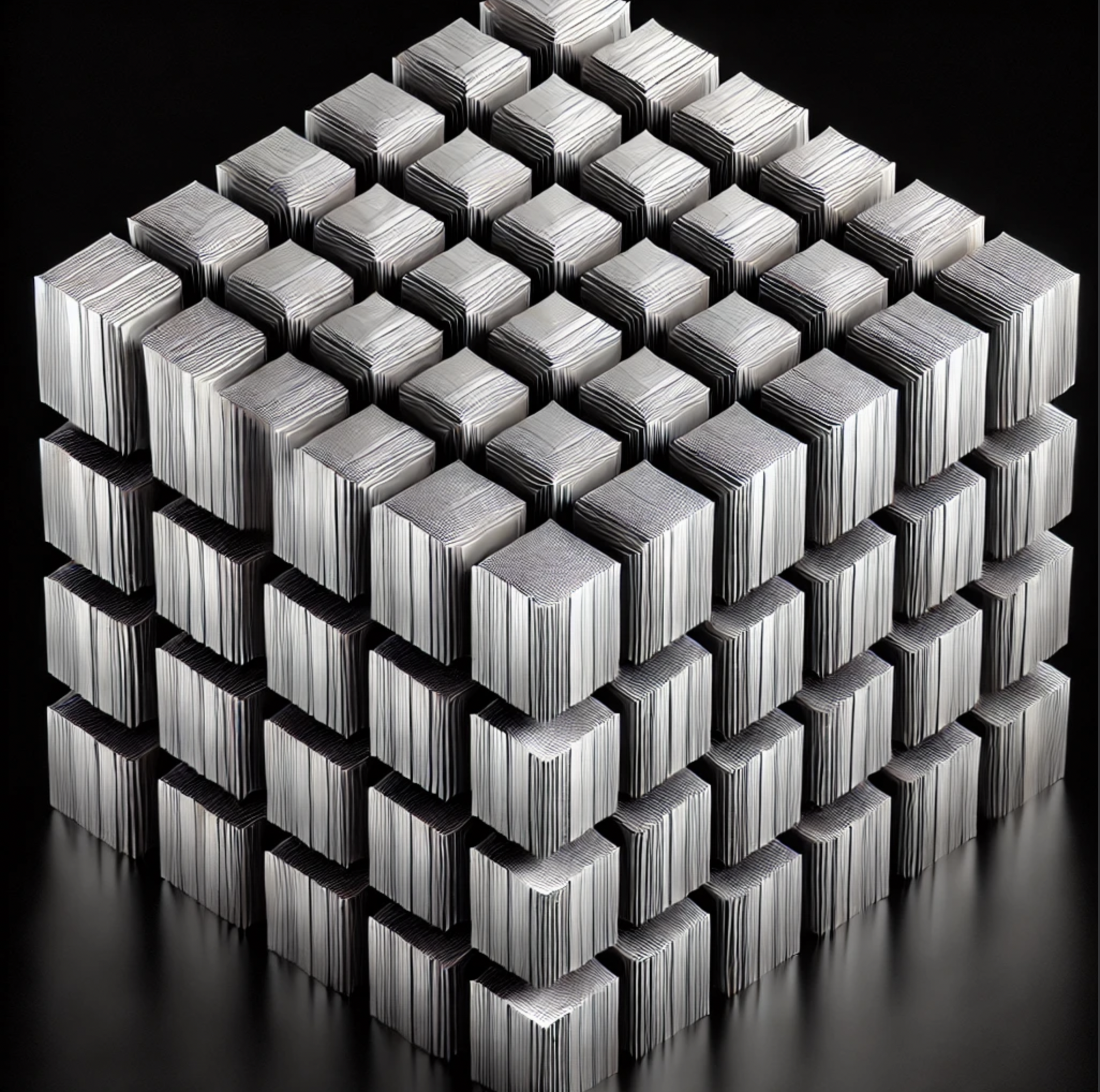
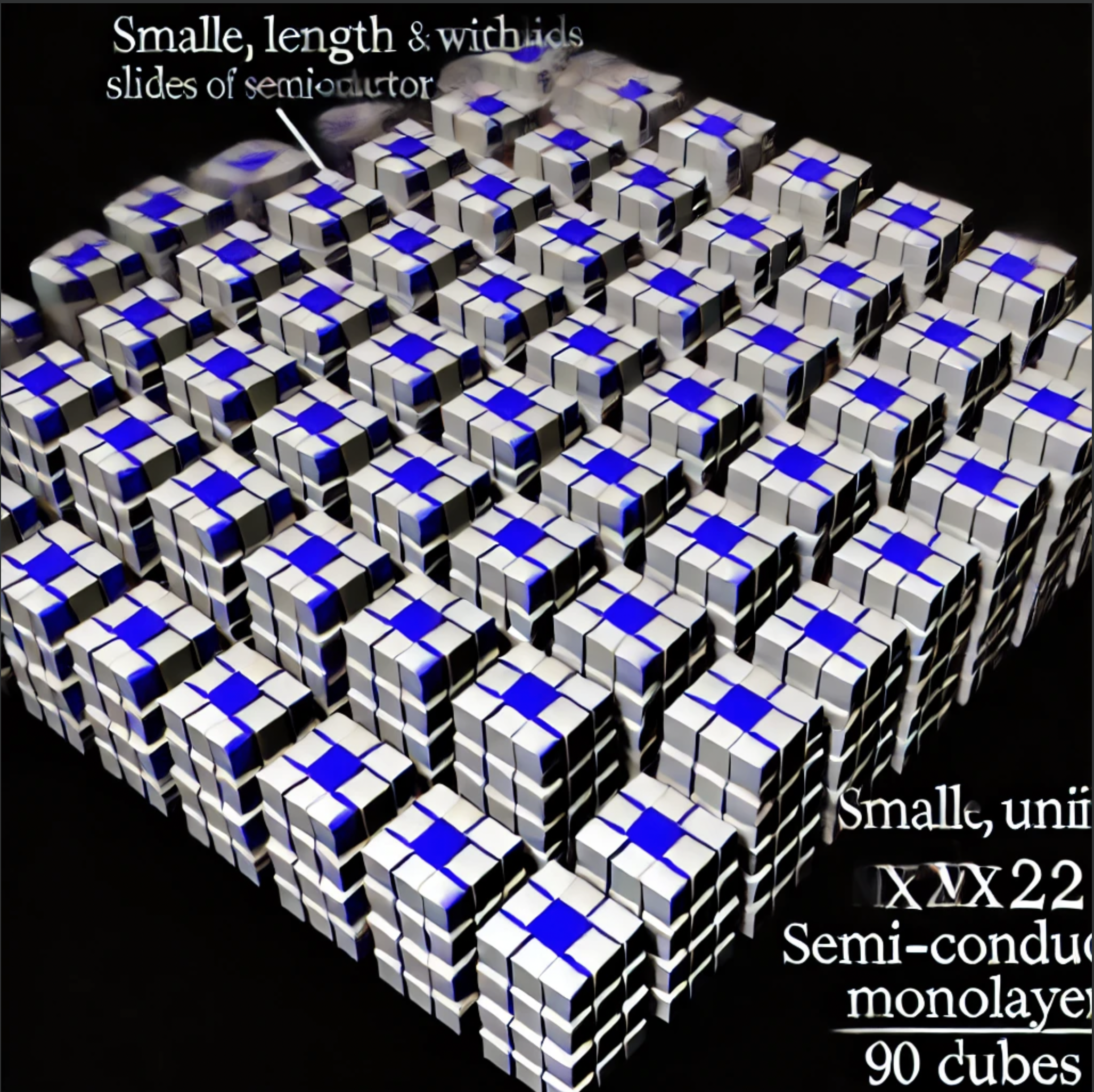
In stacking monolayers into cubed patterns, perhaps rotating cubes for an equality of balancing material properties (isotropy). An example monolayer being 6.5 Å thick (MoS2). With activation potentials being proxy based the right lightware language could balance the gap charges required for initialization and tuning.

Utilizing lightware, to adjust the light intensity, wavelength, or polarization in real-time to tune the electronic properties of the MX2 stacks according to specific needs.

Benefits
- Photonics and Optoelectronics: This configuration could be particularly useful in photonics and optoelectronics, where precise control over light-matter interaction is essential.
- Computational Materials: For computational applications, this setup could allow for the development of highly efficient, light-controlled logic devices or memory storage systems.
- Dynamic Sensors and Actuators: In sensors and actuators, the ability to rapidly modify material properties via light could lead to highly sensitive and responsive systems, adaptable to varying conditions without physical contact or mechanical adjustments.
Application
Electroplating is known to work in creating MX2 monolayers. A miniature ensemble for theoretical conveyer belts of self growing 'lamp socks' with the right programmer of the science of lightware and zyphers.
<= Back
<= Home (Splash)